Memory organization 8051
Memory organization is depends on type of architecture used. There are two type of architectures are used in controller or processor generally : 1) Von Neumann architecture 2) Harvard architecture
- Von Neumann architecture
The term Von Neumann architecture, also known as the Von Neumann model or the Princeton architecture. This architecture consist of address memory and data memory on a single unit . 8085 is based on Von Neumann architecture.
- Harvard architecture
Harvard architecture consist of program memory and data memory as separate unit. Thus for accessing Harvard architecture we need separate address bus, data bus and control bus. 8051 is based on Von Neumann architecture. Hence 8051 consist of two separate memory units, program memory as well as data memory.
Program memory organization :
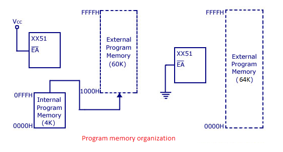
The program memory organization for 8051 family is as shown in fig. above. 8051 microcontroller has an on chip internal program ROM of 4K size and if needed we can add an external memory of size 60K maximum by interfacing. Hence total 64K size memory is available for 8051 microcontroller. By default, the External Access (EA) pin should be connected Vcc its mean that instructions are fetched from internal memory initially. When we cross the internal limit of memory (4K), control of program will automatically goes to external memory and remaining instructions will fetch from external ROM. If we wants only external memory i.e. to fetch instruction from only external memory means if we want bypass internal program ROM, then we have to must connect External Access (EA) pin to ground as shown in fig. above.
Data memory organization :

In the 8051 family, 8051 has total 128 bytes of internal data RAM and we can interface external data memory up to 64K. Hence, total size of data memory in 8051 can be upto external 64K + internal 128 bytes. Internal RAM of 8051 is divided into 3 parts:- 1) Register banks 2) Bit addressable area 3) Scratch pad area.
There are 4 register banks in 8051 bank 0,1, 2 and 3. Each bank has 8 registers of 1 byte R0,R1…R7 respectively. Hence, register banks consist of the lowest 32 bytes of on chip RAM as shown in fig. above. At a time only one register bank can be selected for operations and bank registers are accessed using mnemonics R0..R1.. etc. By default register bank #0 is selected when we reset the system. The bit addressable area is 16 bytes next to register banks. We can access each bit separately of bit addressable area, Each bit have unique address of bit addressable area.The area of bit addressable space of 8051 is usually used to store bit variables. address range 20H to 2FH (total 128 bits) is nothing but bit addressable area as shown in fig. Each bits can be accessed from 00H to 7FH within this 128 bits from 20H to 2FH. Sometimes programming using bit addressable area saves wastage of memory. The upper 80 bytes are nothing but scratch pad area which is used for general purpose storing of data. Scratch pad area is in the address range 30H to 7FH . Scratch pad area can be used for stack memory also if default stack area is insufficient.
There are 4 register banks in 8051 bank 0,1, 2 and 3. Each bank has 8 registers of 1 byte R0,R1…R7 respectively. Hence, register banks consist of the lowest 32 bytes of on chip RAM as shown in fig. above. At a time only one register bank can be selected for operations and bank registers are accessed using mnemonics R0..R1.. etc. By default register bank #0 is selected when we reset the system. The bit addressable area is 16 bytes next to register banks. We can access each bit separately of bit addressable area, Each bit have unique address of bit addressable area.The area of bit addressable space of 8051 is usually used to store bit variables. address range 20H to 2FH (total 128 bits) is nothing but bit addressable area as shown in fig. Each bits can be accessed from 00H to 7FH within this 128 bits from 20H to 2FH. Sometimes programming using bit addressable area saves wastage of memory. The upper 80 bytes are nothing but scratch pad area which is used for general purpose storing of data. Scratch pad area is in the address range 30H to 7FH . Scratch pad area can be used for stack memory also if default stack area is insufficient.


Comments
Post a Comment